 Applications


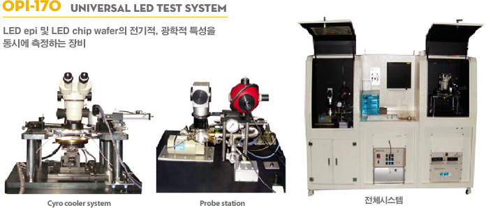
ㆍUniversal LED Tester System consists of Cryo cooler system for controlling extreme temperature and integrating sphere for measuring total Luminous flux ortotal radiation-flux of chip.
ㆍCryo cooler system is a chamber where you can put samples such as a piece of epi and chip wafe, LED unit ,etc and measures optical and electrical property of sample by flexibly changing temperature bewteen 10k~380k [Tempresolving power 0.1 ]
ㆍProbe station measures optical /electrical properties of epi and chip wafer.
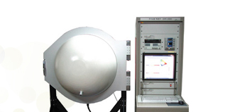
ㆍ6"integrating sphere calculates optical efficacy and measures Total Luminous flux andtotal radiation-flux of chip LED attached to TO can by measuring cryo cooler system and optical power to the change of temperature.
ㆍOptical properties measurement items.
- Spectral properties : Peak wavelength, dominant wavelength, mid-wavelength, center wavelength, Full width half max, color coordinate, purity, color temperature, Color rendering index , etc.
- The amount of lightproperties :Luminance, luminous intensity, intensity radiation, etc.
ㆍElectrical property measuring items.
- forward current, forward voltage, reverse current, reverse voltage, etc.
ㆍSweep measurement items.
- current-voltage, voltage-current, current-optical properties, Temp-Electrical property, and Temp-optical properties.
ㆍMeasure spectral properties using high sensitivity and resolution spectrometer.
ㆍAccurate and stable optical power by correcting color in real time using integrating sphere type input optical system andspectrometer.
ㆍMeasure electrical property using high precision and speed 4 channel source meter.
ㆍMeasure up to 3A of current stressing and print it out in consecutive and pulse format.
ㆍcurrent-voltage, voltage-current, current-optical sweep measurement.
ㆍMeasure optical and electrical properties to change of temperature and time.
ㆍSelect variousFourier domains(UV, UV-VIS, VIS, VIS-IR).
ㆍKeithSelect various power sources (Voltage, current, and pulse) stressing and measurement ranges using Keithley2420 Sourcementer.
ㆍAdditional features available upon user requirements. (Optional)
ㆍSimultaneous measurement of all channels or individual measurement for each channel when measuring multiple chips.
ㆍVarious conditional measurement.
- Repeated Aging Time measurement: Perform one time measurement by repeating the number of times after aging of sample for a certain amount of time.
- Aging Time measurement in certain interval: Perform measurement in certain interval after aging of sample for a certain amount of time.
ㆍThe measurement data is to be saved in a form that allows user to intuitively recognize the change ofoptical properties/electrical property. (CSV file)
ㆍSave data of temperature change over time. (Data and image file)
ㆍSave and open measurement conditions in a form of Project file.
ㆍProvide CIE and KS standard measurement mode.
ㆍCorrect using Korea Research Institute of Standards and Science certified lamp and LED.
ㆍProxy Korea Research Institute of Standards and Science(KRISS) correction certification. (Optional)
ㆍUser oriented set-up and instruction.
ㆍDevelop SW to meet user requirements.
ㆍProvide measurement knowledge and information through activities in CEI and photometry club service and prompt A/S
ㆍRapid A/S
| Specifications | |
| Voltage Range | ±1μV ~ ±105V |
| Current Range | ±100pA to ±3.5A, ±10A[Pulse Only] |
| Setting Temperature | 9K to 390K Resolution 0.1℃ |
| PD Temperature | 20℃ to 30℃ 중 선택, 고정 |
| Spectrometer | 350 to 900nm, 2048 CCD array Type |
| Optical Head | 50mm integrating Sphere |
| Photodiode | 350 to 900nm, 10㎡ Area |
| Dimension | 2,400mm[W] x 1,200mm[D] x 1,800mm[H] |