OPI-160 WAFER-LEVEL LED MEASUREMENT SYSTEM
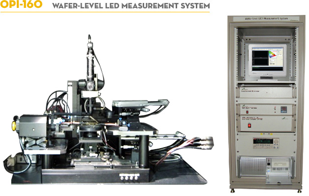
- Easy to measure various items, User interface (Support on-demand SW design)
- ㆍOptical Measurement
- Spectrum, Peak/Dominant wavelength(λp, λd), CIE Color Coordinate(Cx, Cy), Luminous Intensity(cd), Correlated Color Temperature(CCT(Tc)), Color Rendering Index(CRI(Ra)), CIE XYZ(), Radiant Flux(mW), Luminous Flux(lm), Spatial Intensity Distribution(IES, LDT)
- ㆍElectrical Measurement
- Forward/ Reverse Current[lf, lr], Forward/Reverse Voltage[Vf, Vr], l-V-L Sweep
- ㆍTemperature Dependence Measurement
- Temperature.VS.Electrical/optical Test
- ㆍCurrent Spreading and Degradation Analysis
- Real time Image analysis of LED using CCD Camera and beam profiler software
- Optimized for R&D
-
ㆍ Integrated measurement of optical, electrical and thermal dependency required in wafer level.
-
ㆍ Automation of measurement and convenient user environment.
-
ㆍ Observation of Chip Current spreading and degradation using high resolution microscope and camera.
-
ㆍ Function integration and verification by a number of reseachers.
-
ㆍ Provide CIE measurement mode andKRISS standard value.
-
ㆍ High precision measurement using Keithley 2612
-
ㆍ Low noise and high precision / reproduction using TE Cooled 2048 pixel CCD sensor.
-
ㆍ Display light distribution characteristics in 2D/3D graphs and data list by analyzing, summarizing and duplicating measured data.